
Description
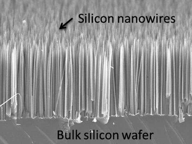
Silicon nanowire arrays have been utilized in a variety of applications, including Li-ion batteries, solar cells, optical coatings, microfluidics, biosensing and photocatalysis. These materials are especially well-suited for applications that require large surface areas and could take advantage of the broader silicon know-how.
| PARAMETER | AVAILABLE RANGE** | STANDARD PRODUCTS* |
|---|---|---|
| Process & Material | visit Si Nanowires Technology page | Si, without residual Ag catalyst |
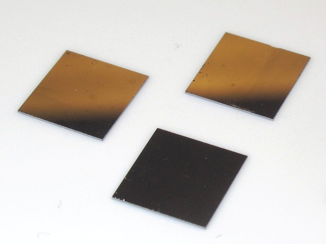
| Nanowire diameter, nm | 75 – 600 | 200 ± 50
(target value, trending lower for length ≥5 µm) |
| Nanowire Length, µm | 0.1 – 10 | 0.5, 1, 2, 3, 5 (±50%) |
| Fill Fraction, % | 10 – 45 | 25 – 30 |
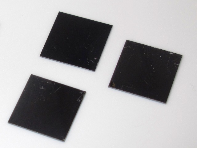
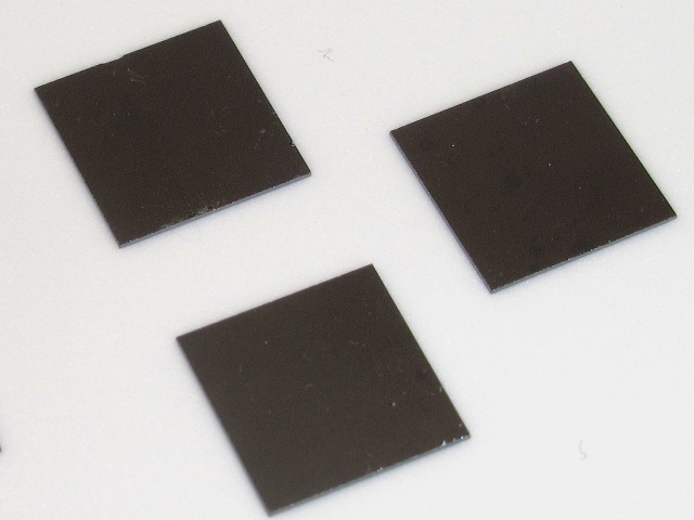
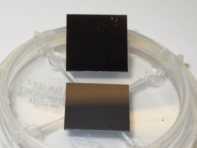
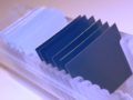
| Substrate Size, mm | up to 50 mm Si wafer | 10 x 10 |
| Substrate Type | Si wafers, poly Si on different substrates | prime grade Si <100> wafers, p-type, 1-10 Ohm-cm |
* Lead time for standard specifications is 2 – 3 days. Due to limited inventory, some of the standard specifications may be temporarily out of stock. Lead time for out of stock and custom specifications s 3-6 weeks.
** For availability of Si nanowires with custom specifications, contact us with your requirements.
*** Volume discounts are available in quantities over 20 substrates.
Products are designed and fabricated by InRedox partner, Advanced Silicon Group, a global leader in silicon nanotexturing and its applications, pat. http://www.advancedsilicongroup.com/patents.html.
 InRedox