Silicon Nanowire Arrays

How Si Nanowires Are Made

Silicon nanowire arrays or SiNWs are vertically aligned arrays of silicon nanowires on a planar crystalline silicon wafer substrate.  These nanowires are made by a catalytic oxidation and dissolution of Si in the presence of metal catalyst nanoparticles – a self-organized process commonly referred to as metal enhanced etching, metal assisted chemical etching (MACE), or metal assisted etching (MAE) .  This process has been known for many decades (Li, Bohn, Appl. Phys. Lett. 77, 2572 (2000)).

InRedox’s partner, Advanced Silicon Group, have innovated on the MACE processes to make resulting Si Nanowire arrays more reproducible and uniform, and to allow the properties of the nanowires to be tuned.

The MACE process always involves deposition of a metal and etching in a solution containing hydrofluoric acid (HF) and an oxidizer.  The silicon is etched only where the metal nanoparticle touches the silicon, as a result of coupled electrochemical reactions mediated by the nanoparticle.  As the silicon is etched, the nanoparticles move into the resulting nanopores.  Since the silicon is only etched locally, the process can result in features with very high aspect ratio.

Metal assisted chemical etching of silicon (MACE)

The process can be tuned by adjusting the following parameters:

  • Type of metal
  • Deposition method of metal
  • Preparation of the silicon surface prior to metal deposition
  • Treatment of the metal before etching
  • Chemistry of the etching solution
  • Parameters during the etching process
  • Type of oxidizer used in the etching process

For more information on the MACE process see review by Toor, Black et al,  Nanotechnology 27, 412003 (2016).

Si Nanowire Arrays Products

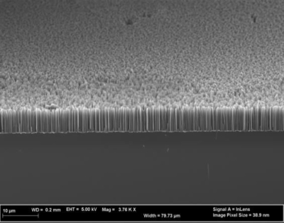
Arrays of Si nanowires based on this technology are now offered by InRedox through a partnership with Advanced Silicon Group (ASG).


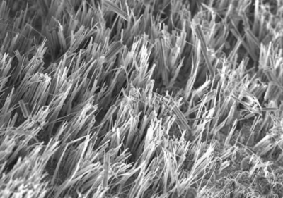
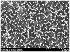
Typical SEM images of Si nanowire arrays produced by ASG.

Properties of Si Nanowires

MACE results in Si nanowire arrays with unique attributes as compared to other fabrication techniques:

  • Single crystalline
  • High aspect ratio, vertically aligned
  • Large surface area to volume ratio
  • Uniform diameter and lengths
  • Uniform doping throughout the nanowires
  • Variable density

Applications of Si Nanowires

  • Sensors
    Nanowires with high surface to volume ratio have the potential to make high sensitivity detectors.  Silicon has been functionalized to be sensitive to many different materials including proteins and specific DNA.
  • Anodes for Lithium ion batteries
    Silicon has the highest known capacity of any Li-ion battery anode material.  Unfortunately, bulk silicon expands and contracts 4x with charge/discharge cycles.  Therefore, bulk silicon can only cycle a handful of times before it essentially pulverizes, making the battery unusable.  Nanostructured silicon can expand and contract while retaining its structural integrity.  Nanowires allow the expansion and contraction of the crystal lattice in two dimensions while still providing a conductive path to the electrode in the third dimension.
  • Low reflective surfaces
    Since nanowires are smaller than the wavelength of light, light incident onto the silicon surface sees a composite of the silicon and the material around it (for example air).  This leads the light to see an index of refraction that is between that of air and that of silicon.  The graded index of refraction of silicon nanowire arrays can lead to a very low reflection for a wide range of wavelengths and angles for incident light.
  • Photovoltaics
    Black or nanotextured silicon can improve the efficiency and lower the cost of silicon solar cells. For more information on this application see the review article by Toor, Black et al, Nanoscale 8, 15448-15466 (2016).
  • Thermoelectric devices
    Silicon nanowires have been are able to scatter phonons effectively while having a low electrical resistance, resulting in a high theremoelectric figure of merit.  For more information on see for example Yang et al, Nature 451, 163-167 (2008).