• LinkedIn
  • Youtube
  • Skype
  • Pinterest
  • Login
  • Contact
  • 0Shopping Cart
InRedox
  • About
    • Management Team
    • News
    • Customers’ Publications
    • Contact Us
  • Technology
    • Anodic Aluminum Oxide
    • Anodic Titanium Oxide
    • Atomic Layer Deposition
    • Silicon Nanowire Arrays
    • Ceramic Microdevices
      • High Temperature Pressure Sensors
  • Applications
    • Templated Nanofabrication
    • Anodic Alumina in Graphene Synthesis
    • Cell Culturing on Nanostructured Substrates
    • Photocatalysis with Anodic Titanium Oxide Nanotubes
    • UV-induced super-hydrophilicity in Anodic Titanium Oxide
  • Products
    • Nanofabrication Toolbox
      • AAO Wafers & Packs
        • AAO Wafers
        • AAO Wafers with Contacts
        • AAO Variety Packs
        • AAO Volume Packs
      • AAO and ATO Nanotemplates
        • AAO Films on Al
        • AAO Films on Substrates
        • ATO Films on Ti Foil
      • Accessories
        • Holder for Electrodeposition
        • Tweezers for AAO Wafers
        • Replacement Parts
    • Nanoarrays and Coatings
      • AAO-ALD Nanocomposites
        • AAO Wafers with ALD Coatings
        • AAO Films with ALD Coatings
      • Silicon Nanowire Arrays
    • Filtration and Separation
      • Isotropic AAO Membranes
      • Anisotropic AAO Membranes
      • AAO Membrane Holders
      • Tweezers for AAO Membranes
    • Life Science Products
      • AAO Cell Culture Substrates
      • ATO Cell Culture Substrates
      • Filters & Membranes
  • Support
    • Inquiry Form
    • Frequently Asked Questions
    • Customers’ Publications
  • Store
    • Terms and Conditions
    • Cart
    • Checkout
    • My Account
  • Search
  • Menu Menu
Shop
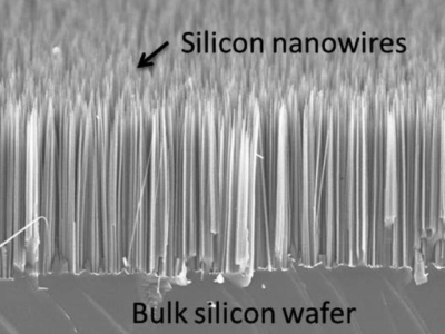
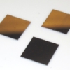
Arrays of Si nanowires on Si wafer
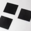
Array of ~3 um long Si nanowires on 10 mm x 10 mm Si substrates
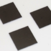
Array of 1 um long Si nanowires on 10 mm x 10 mm Si substrates
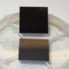
Array of 0.5 um and 3 um long Si nanowires on 10 mm x 10 mm Si substrates
Array of 0.5 um long Si nanowires on 10 mm x 10 mm Si substrates

Silicon Nanowire Arrays

$0.00 – $395.00

Vertically aligned arrays of high aspect ratio high density Si nanowires on Si wafers are prepared using metal-assisted chemical etching of silicon (MACE).  These arrays could be made over large areas, with adjustable diameter, density, and length of the nanowires.  A thin layer of catalytic metal remaining at the base of the nanowires can be removed by selective etching.  Standard offerings currently include:

•   Pack of 3 of 1 cm x 1 cm pieces of Si wafer with nanowires on one face,
•   One nanowire diameter (200 nm),
•   Three nanowire lengths (0.5, 1 and 3 µm) are in stock,
•   Longer nanowires (5 and 10 µm) are under development.

To purchase standard product, select the specifications from the menu below and click add to cart.  For other nanowire geometries and substrates, contact us with your requirements

Clear
SKU: SiNW-SIZE-DIA-LENGTH Category: Si Nanowires Tag: Si Nanowires
  • Description
  • Additional information

Description

Silicon nanowire arrays have been utilized in a variety of applications, including Li-ion batteries, solar cells, optical coatings, microfluidics, biosensing and photocatalysis. These materials are especially well-suited for applications that require large surface areas and could take advantage of the broader silicon know-how.
PARAMETER AVAILABLE RANGE** STANDARD PRODUCTS*
Process & Material visit Si Nanowires Technology page Si, with or without residual Ag catalyst
Nanowire diameter, nm 75 – 600 200 ± 50
Nanowire Length, µm 0.1 – 100 0.5,  1, 3 (±50%)
Fill Fraction, % 10 – 45 25 – 30
Substrate Size, mm up to 50 mm Si wafer 10 x 10
Substrate Type Si wafers, poly Si on different substrates prime grade Si <100> wafers, p-type, 1-10 Ohm-cm
* Current lead time for standard specifications is 2-3 weeks.
** Custom Si nanowire arrays are available upon request. Contact us with your requirements.
*** Volume discounts are available in quantities over 20 substrates.
Products are designed and fabricated by InRedox’s partner, Advanced Silicon Group, a global leader in silicon nanotexturing and its applications, pat.  http://www.advancedsilicongroup.com/patents.html.

Additional information

Dimensions 10 × 10 × 0.28 mm
Size & Qty

3 pcs of 1 cm x 1 cm, inquire for other sizes

Si NW diameter

200±50 nm

Si NW length

0.5 µm, 1.0 µm, 3.0 µm

Contact

1-720-295-9102
info@inredox.com

1840 Skyway Drive, Unit F
Longmont, CO 80504 USA

Product Categories

  • Nanofabrication Toolbox
  • Nanoarrays and Coatings
  • Filtration and Separation
  • Life Science Products

Quick Links

  • Request a Quote
  • Technical Inquiry
  • Frequently Asked Questions
  • Terms and Conditions
  • My Account
InRedox LLC © 2011-2017 | All Rights Reserved
  • LinkedIn
  • Youtube
  • Skype
  • Pinterest
AAO Films with ALD Coatings 25 mm x 25 mm AAO nanotemplates with ALD coatings Tweezers for AAO Handling
Scroll to top